- 您现在的位置:买卖IC网 > Sheet目录479 > MRF89XA-I/MQ (Microchip Technology)TXRX ISM SUB-GHZ ULP 32QFN
MRF89XA
2.4.4
IF GAIN AND SECOND I/Q MIXER
2.5
Frequency Synthesizer Block
Following the LNA and first down-conversion, there is
an IF amplifier whose gain can be programmed from
13.5-0 dB in 4.5 dB steps, through the register
DMODREG. For more information, refer to
Section 2.14.2, DATA AND MODULATION
CONFIGURATION REGISTER DETAILS . The default
setting corresponds to 0 dB gain, but lower values can
be used to increase the RSSI dynamic range.
2.4.5 CHANNEL FILTERS
The second mixer stages are followed by the channel
select filters. The channel select filters have a strong
influence on the noise bandwidth and selectivity of the
receiver and therefore, its sensitivity. Each channel
select filter features a passive second-order RC filter,
with a programmable bandwidth and the “fine” channel
selection is performed by an active, third-order,
Butterworth filter, which acts as a low-pass filter for the
zero-IF configuration (FSK), or a complex polyphase
filter for the low-IF (OOK) configuration. For more
information on configuring passive and active filters
see Section 3.4.4, Channel Filters .
The frequency synthesizer of the MRF89XA is a fully
integrated integer-N type PLL. The crystal oscillator
provides the reference frequency for the PLL. The PLL
circuit requires only a minimum of five external
components for the PLL loop filter and the VCO tank
circuit.
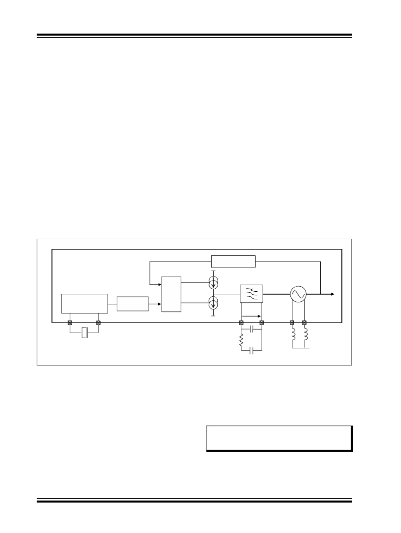
Figure 2-4 illustrates a block schematic of the
MRF89XA PLL. Here the crystal reference frequency
and the software controlled dividers R, P and S blocks
determine the output frequency of the PLL.
The VCO tank inductors are connected on an external
differential input. Similarly, the loop filter is also located
externally.
FIGURE 2-4:
MRF89XA
XO
FREQUENCY SYNTHESIZER BLOCK DIAGRAM
÷ 75 * (Pi + 1) + Si
PFD
÷ (Ri + 1)
LO
F COMP
Vtune
OSC1
OSC2
PLLP
PLLN
VCOTP
VCOTN
VCORS
2.5.1
REFERENCE OSCILLATOR PINS
Choosing a higher tolerance crystal results in a lower
(OSC1/OSC2)
The MRF89XA has an internal, integrated oscillator
circuit and the OSC1 and OSC2 pins are used to
connect to an external crystal resonator. The crystal
oscillator provides the reference frequency for the PLL.
The crystal oscillator circuit, with the required loading
TX to RX frequency offset and the ability to select a
smaller deviation in baseband bandwidth. Therefore,
the recommended crystal accuracy should be ≤ 40
ppm. The guidelines for selecting the appropriate
crystal with specifications are explained in Section 4.6,
Crystal Specification and Selection Guidelines .
capacitors, provides a 12.8 MHz reference signal for
the PLL. The PLL then generates the local oscillator
frequency. It is possible to “pull” the crystal to the
accurate frequency by changing the load capacitor
value. The crystal oscillator load capacitance is
typically 15 pF, which allows the crystal oscillator circuit
to accept a wide range of crystals.
Note:
Crystal frequency error will directly trans-
late to carrier frequency (f rf ), bit rate and
frequency deviation error.
DS70622C-page 16
Preliminary
? 2010–2011 Microchip Technology Inc.
发布紧急采购,3分钟左右您将得到回复。
相关PDF资料
MRF89XAM9A-I/RM
IC TXRX MOD 915MHZ ULP SUB-GHZ
MRX-001-433DR-B
MODULE RECEIVER 433MHZ 18DIP
MRX-002-433DR-B
MODULE RECEIVER 433MHZ 18DIP
MRX-002SL-433DR-B
MODULE RCVR 433MHZ SAW LN 24DIP
MRX-005-915DR-B
MODULE RECEIVER 915MHZ 18DIP
MRX-005SL-915DR-B
MODULE RCVR 915MHZ SAW LN 24DIP
MRX-007-433DR-B
MODULE RECEIVER 433MHZ 18DIP
MRX-008-433DR-B
MODULE RECEIVER 433MHZ 18DIP
相关代理商/技术参数
MRF89XAM8A-I
制造商:MICROCHIP 制造商全称:Microchip Technology 功能描述:Ultra Low-Power, Integrated ISM Band Sub-GHz Transceiver
MRF89XAM8A-I/RM
功能描述:射频模块 868MHz Sub-GHz transceiver module
RoHS:否 制造商:Linx Technologies 产品:Transceiver Modules 频带:902 MHz to 928 MHz 输出功率:- 15.5 dBm to + 12.5 dBm 接口类型:UART 工作电源电压:- 0.3 VDC to + 5.5 VDC 传输供电电流:38.1 mA 接收供电电流:22.7 mA 天线连接器类型:U.FL 最大工作温度:+ 85 C 尺寸:1.15 mm x 0.63 mm x 0.131 mm
MRF89XAM8A-I/RM
制造商:Microchip Technology Inc 功能描述:, Leaded Process Compatible:Yes, Peak Re
MRF89XAM9A_12
制造商:MICROCHIP 制造商全称:Microchip Technology 功能描述:915 MHz Ultra Low-Power Sub-GHz Transceiver Module
MRF89XAM9A-I/RM
功能描述:射频模块 915MHz Sub-GHz Transceiver Mod RoHS:否 制造商:Linx Technologies 产品:Transceiver Modules 频带:902 MHz to 928 MHz 输出功率:- 15.5 dBm to + 12.5 dBm 接口类型:UART 工作电源电压:- 0.3 VDC to + 5.5 VDC 传输供电电流:38.1 mA 接收供电电流:22.7 mA 天线连接器类型:U.FL 最大工作温度:+ 85 C 尺寸:1.15 mm x 0.63 mm x 0.131 mm
MRF89XAM9AT-I/RM
制造商:Microchip Technology Inc 功能描述:915 MHz Ultra Low-Power Sub-GHz Transceiver Module
MRF89XAT-I/MQ
功能描述:射频收发器 868/915/950 MHz Sub-GHz transceiver RoHS:否 制造商:Atmel 频率范围:2322 MHz to 2527 MHz 最大数据速率:2000 Kbps 调制格式:OQPSK 输出功率:4 dBm 类型: 工作电源电压:1.8 V to 3.6 V 最大工作温度:+ 85 C 接口类型:SPI 封装 / 箱体:QFN-32 封装:Tray
MRF8HP21080HR3
功能描述:射频MOSFET电源晶体管 HV8 2.1GHZ 160W NI780H-4 RoHS:否 制造商:Freescale Semiconductor 配置:Single 晶体管极性: 频率:1800 MHz to 2000 MHz 增益:27 dB 输出功率:100 W 汲极/源极击穿电压: 漏极连续电流: 闸/源击穿电压: 最大工作温度: 封装 / 箱体:NI-780-4 封装:Tray
